
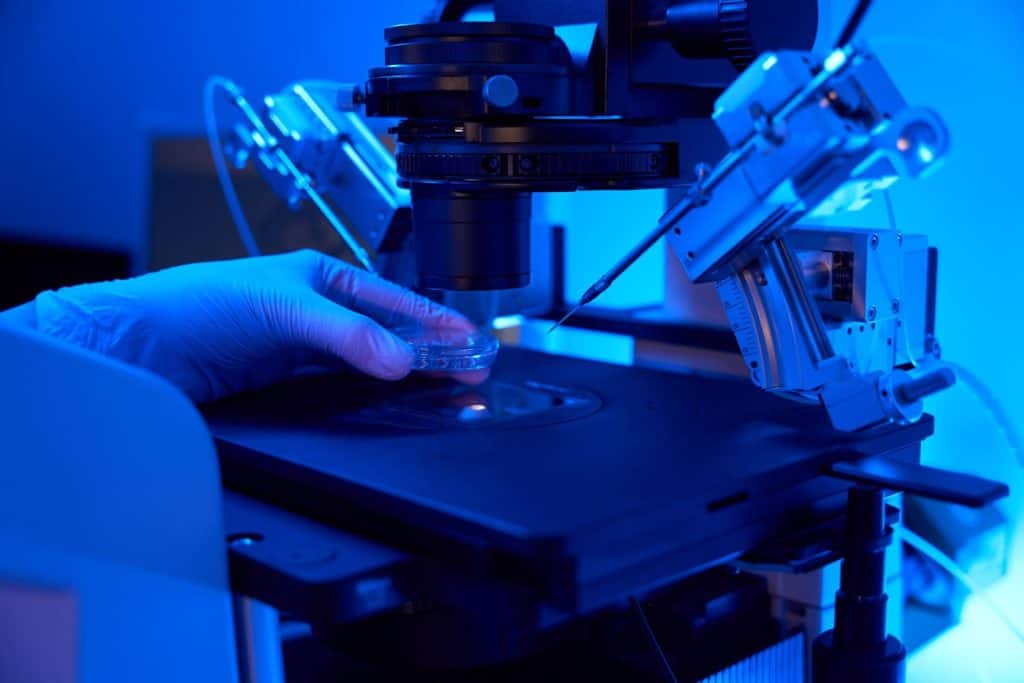
When a critical industrial component fails during operation or mass production, relying on standard visual inspection is rarely sufficient. Engineers must examine the material at the micro and nano levels to understand the exact mechanism of degradation. The most effective diagnostic method for this task is scanning electron microscopy (SEM). By utilizing a focused beam of high energy electrons instead of light, this advanced imaging technology provides incredible depth of field and extreme magnification, allowing scientists to observe the microscopic topography of any solid sample.
In the realm of failure analysis, this tool acts as the ultimate investigative asset. It transitions the engineering team from guessing why a product broke to knowing exactly how the fracture propagated or where the chemical contamination originated.
Key Industrial Applications for Defect Resolution
The ability to accurately visualize microscopic anomalies makes this analytical technique a critical requirement for quality assurance teams across diverse manufacturing sectors.
- Medical Device Manufacturing: Implantable devices, such as titanium joints or cardiovascular stents, must have flawless surfaces. Analysts utilize this equipment to detect microscopic burrs, surface impurities, or early signs of localized corrosion that could endanger patient safety.
- Automotive and Aerospace Engineering: Metal fatigue is a major concern for moving mechanical parts. When a gear or turbine blade fractures unexpectedly, engineers examine the break point to identify fatigue striations, cleavage facets, or micro structural voids, determining if the failure was due to a design flaw or poor casting.
- Polymer and Advanced Composites: Beyond metals, SEM is heavily utilized to inspect plastic components and carbon fiber composites. It helps identify issues like polymer delamination, poor filler dispersion, or environmental stress cracking caused by chemical exposure.
Resolving manufacturing defects rapidly is crucial to minimizing downtime and protecting brand reputation. By incorporating professional scanning electron microscopy analysis into their quality control protocols, companies can gather the irrefutable visual evidence needed to correct their production lines. To ensure maximum accuracy and independent verification, proactive manufacturers consistently partner with an Alstesting Laboratory Testing service in Malaysia to secure their supply chains against hidden material flaws.
Frequently Asked Questions (FAQ)
How does SEM help specifically in root cause failure analysis?
It provides ultra high resolution images of a fracture surface or defective area. By studying the microscopic topography, metallurgists and material scientists can read the “fingerprints” of the failure, determining whether it was caused by brittle overload, ductile tearing, fatigue, or stress corrosion cracking.
Can SEM be used to analyze non metallic materials like plastics?
Yes, it is highly effective for analyzing polymers, plastics, and ceramics. However, because these materials do not naturally conduct electricity, they are usually sputter coated with an ultra thin, microscopic layer of conductive metal (like gold) before being placed under the electron beam to prevent image distortion.
What is the role of EDX in conjunction with SEM testing?
While the electron beam provides the visual image of the sample, an attached Energy Dispersive X-ray (EDX) detector measures the X-rays bouncing off the material. This combination allows the laboratory to not only see a microscopic contaminant but also instantly identify its exact chemical and elemental composition.